User Rizky92 uploaded the image
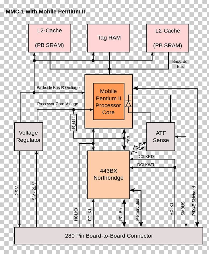
A block diagram of a mobile pentium II processor core. It consists of four components: L2-Cache (PB SRAM), Tag RAM (Tag RAM), and ATF Sense (ATF Sense). The main component of the processor is the Mobile Pentium II Processor Core, which is a mobile processor with a capacity of 443BX Northbridge. The processor is connected to a voltage regulator, which helps to regulate the voltage of the voltage regulator. There are also two other components in the block diagram - the L2 Cache (pb SRAM) and the Tag RAM. The Tag RAM is a type of RAM that is used to store and transfer data from one device to another. The voltage regulator is a device that allows the user to control the voltage and current in the processor, while the ATF sense is a sensor that detects the current and voltage levels in the device. - The 480 Pin Board-to-Board Connector is also used to connect the two components together.
Back-side Bus Intel Front-side Bus Central Processing Unit PNG
. The resolution of this PNG file is 842 x 1024 pixels and it has a file size of 66.64 KB.A block diagram of a mobile pentium II processor core. It consists of four components: L2-Cache (PB SRAM), Tag RAM (Tag RAM), and ATF Sense (ATF Sense). The main component of the processor is the Mobile Pentium II Processor Core, which is a mobile processor with a capacity of 443BX Northbridge. The processor is connected to a voltage regulator, which helps to regulate the voltage of the voltage regulator. There are also two other components in the block diagram - the L2 Cache (pb SRAM) and the Tag RAM. The Tag RAM is a type of RAM that is used to store and transfer data from one device to another. The voltage regulator is a device that allows the user to control the voltage and current in the processor, while the ATF sense is a sensor that detects the current and voltage levels in the device. - The 480 Pin Board-to-Board Connector is also used to connect the two components together.
Back-side Bus Intel Front-side Bus Central Processing Unit PNG
You might also like...